
Semiconductor Scaling Map
Explore the world with this free Semiconductor Scaling Map. Ideal for classrooms, travel planning, or geography projects — available in standard printable sizes. Download instantly and print as many copies as you need.
How to Use This Semiconductor Scaling Map
- Browse the collectionScroll through the Semiconductor Scaling Map designs above and click any image to open it full size.
- Download the imageHit the Download button to save the full-resolution file to your device.
- Print on standard paperUse A4 or Letter paper. Select 'Fit to page' in your printer settings to ensure nothing is cut off.
- Use immediatelyNo editing, software, or account needed — it's ready the moment it comes out of the printer.
More Semiconductor Scaling Map Templates
 Engineer Wikipedia
 Semiconductor To Know More Cantier Systems
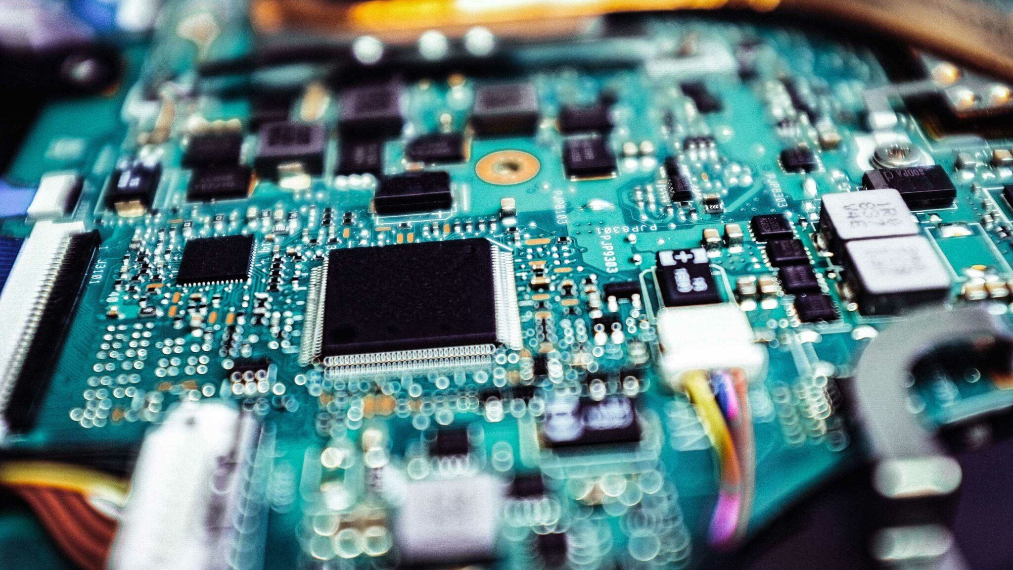 India Semiconductor Mission Incentives For Development Of
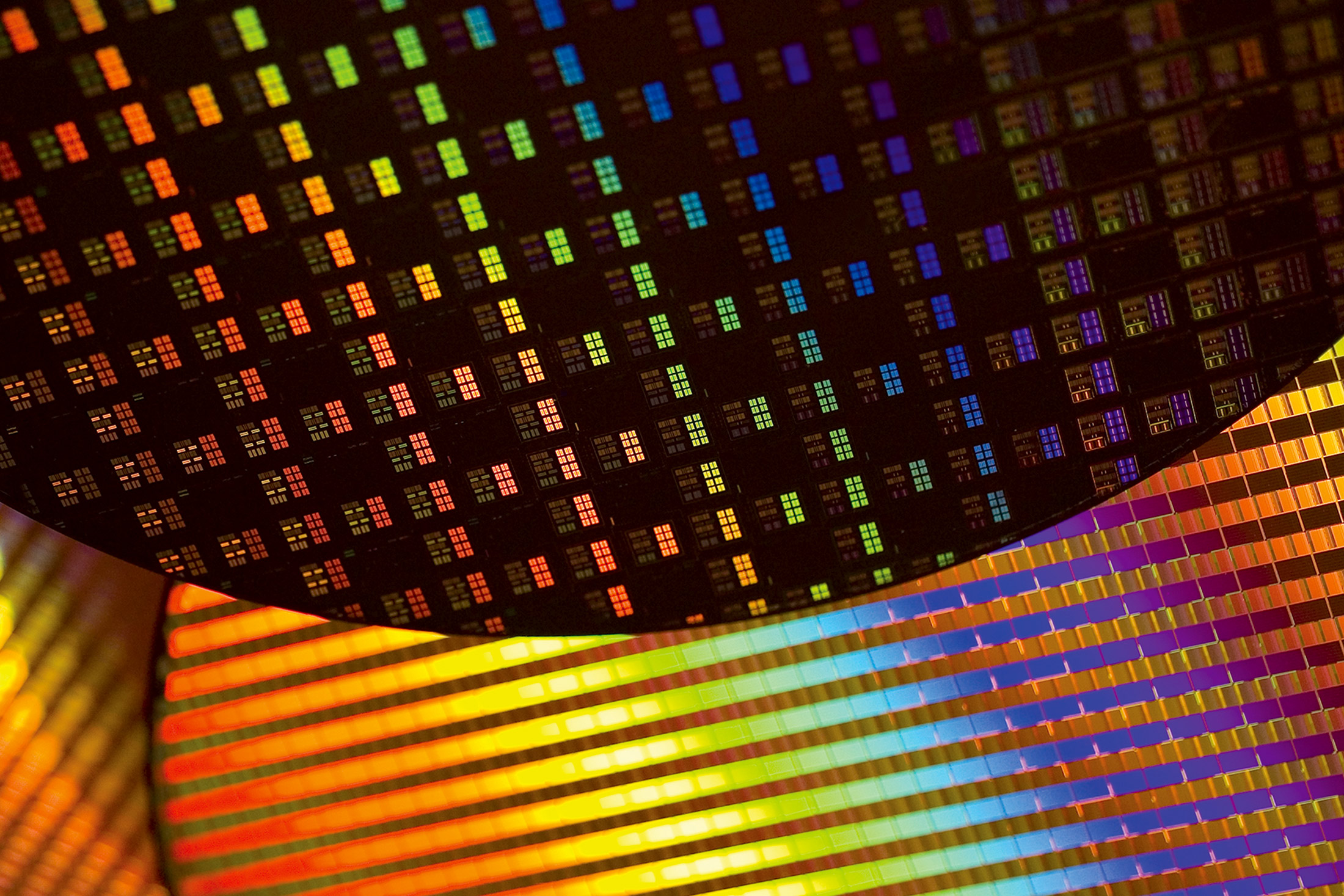 The World Is Dangerously Dependent On Taiwan For Semiconductors Bloomberg
 Machine Learning Subject Matter Experts In Semiconductor Manufacturing KX
 Reflecting On Semiconductor Manufacturing Stocks Q1 Earnings Lam
 Factory Uses Of Semiconductor Materials With The Best Materials
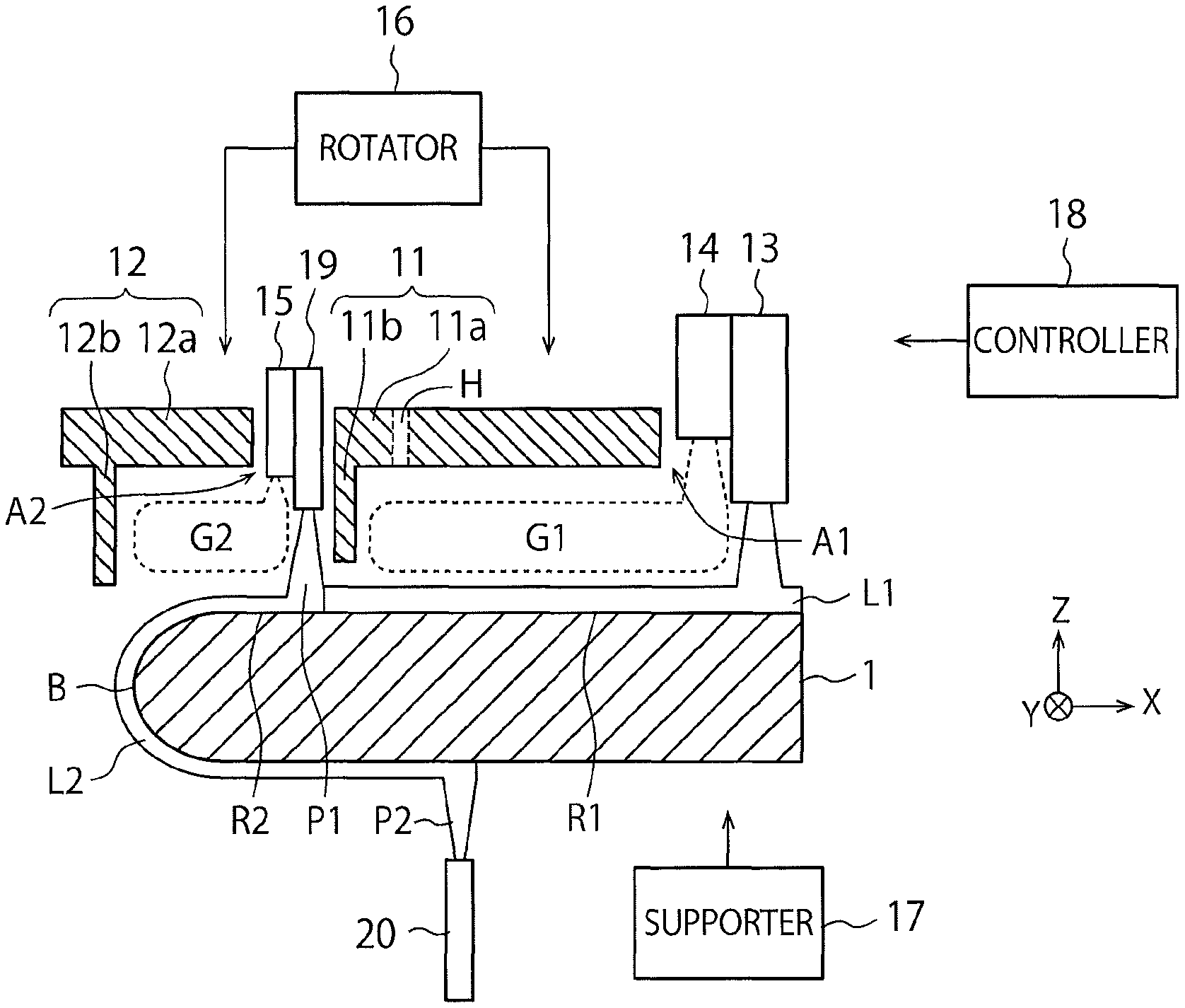 Semiconductor Manufacturing Apparatus And Method Of Manufacturing
 Semiconductors Boost Manufacturing With Specialist Supply Chain
 Swiggy s Delivery Staff Strike Again VCs On Wait Mode Govt Scrutiny
 Semiconductor Industry Statistics Facts And Trend
 The Semiconductor Manufacturing Cluster chetanpatil Chetan Arvind
 PDF 2017 Electronic Semiconductor Manufacturing
 Japan Bolsters Its Chip Industry With Buyout Of Equipment Maker JSR
 Semiconductor Process Engineer Job Description Velvet Jobs
 Semiconductor Manufacturing Pdf Jacksonnew
 A New Undergraduate Semiconductor Manufacturing Option In The Chemical
 Semiconductor Technician Resume Tawaheltub
 The Automated World Of Semiconductor Manufacturing chetanpatil
 How Many Types Of A4 Paper Are There Printable Templates Free
 UK Unveils 1bn Semiconductor Strategy
 PDF Semiconductor Manufacturing DOKUMEN TIPS
 Semiconductor Industry Archives Al Awais Movers
 Semiconductor Manufacturing Device And Method Eureka Patsnap
 PDF Case Study On A Semiconductor Manufacturing Company
 Semiconductor Manufacturing Plant Seamless Vector Image
 ASE SemiconductorSemiconductor Scaling Map
 Investing In AI With Semiconductor Stocks BusinessCircle
 Semiconductor Structure And Fabrication Method Thereof Patent Grant
 Semiconductor Manufacturing Electronic Graphic By Frogella stock
 Semiconductor Manufacturing Technology
  Semiconductor Manufacturing Attracts Global Firms Ashwini Vaishnaw
 Semiconductor Shanghai Miandi Metal Group Co Ltd
 Frequently Asked Questions
Is this Semiconductor Scaling Map free to use?
Yes, 100% free. Download and print without creating an account or providing your email address.
What paper size does this template support?
Templates are designed for A4 and US Letter paper. Select 'Fit to page' in your printer dialog for the best fit.
Can I print multiple copies?
Yes. Once you download the image, you can print it as many times as you like for personal or educational use.