DEVICE MODELING
Download this free DEVICE MODELING and use it right away. Optimized for A4 and Letter paper, all 100 designs are ready to print without editing software. No sign-up required.
How to Use This DEVICE MODELING
- Browse the collectionScroll through the DEVICE MODELING designs above and click any image to open it full size.
- Download the imageHit the Download button to save the full-resolution file to your device.
- Print on standard paperUse A4 or Letter paper. Select 'Fit to page' in your printer settings to ensure nothing is cut off.
- Use immediatelyNo editing, software, or account needed — it's ready the moment it comes out of the printer.
More Device Modeling Templates
 VLSI Beginner Laptop Desktop Configuration ? QnA ! - YouTube
 Difference : Simulation Vs Emulation in VLSI ? QnA ! - YouTube
 VLSI QnA: Digital Design Interview Questions - v1.2
 What to Learn to Enter into the VLSI Industry ? Learning for VLSI | QnA | EP-6 - YouTube
 VLSI JOBs inside Digital Design Domain (ASIC & FPGA) ! QnA | EP-8 PART-I - YouTube
 You Don't Know How To Job Switch From IT-Software to VLSI ? - YouTube
 You Don't Know About Isolation Cell from Standard Cell Library in VLSI ? - YouTube
 Fresher New Joinee In VLSI Career Growth ? Campus OR Off Campus Recruitment ! QnA - YouTube
 Top 50+ Interview Questions And Answers On VLSI CMOS Circuits
 You Don't Know About Standard Cell Library in VLSI ? - YouTube
 VLSI QnA - Digital Design Interview Questions - v1.3 Q.1)... | Facebook
 From PCB-Design to VLSI-Design Career Change ? Possible or Not ? QnA ! - YouTube
 You Don't Know About Indispensable Linux Commands in VLSI LIVE DEMO - YouTube
 Low Power Design – VLSI System Design
 12 Knowledge About VLSI ideas | knowledge, interview questions, classroom solutions
 Events – VLSI System Design
 UVM the Universal Verification Methodology | Facebook
 Synopsys #vlsi Analog Devices & Synopsys Interview Experience with Sonalika Singh || QnA - YouTube
 Ecosystem of VLSI Companies Worldwide | VLSI Ecosystem | What is VLSI Industry ? - YouTube
 What is AWK Programming ? BASH Programming in VLSI | Episode-4 - YouTube
 STA | VLSI Design Live Analysis in OpenTimer STA | EP-4 | QnA | TCL - YouTube
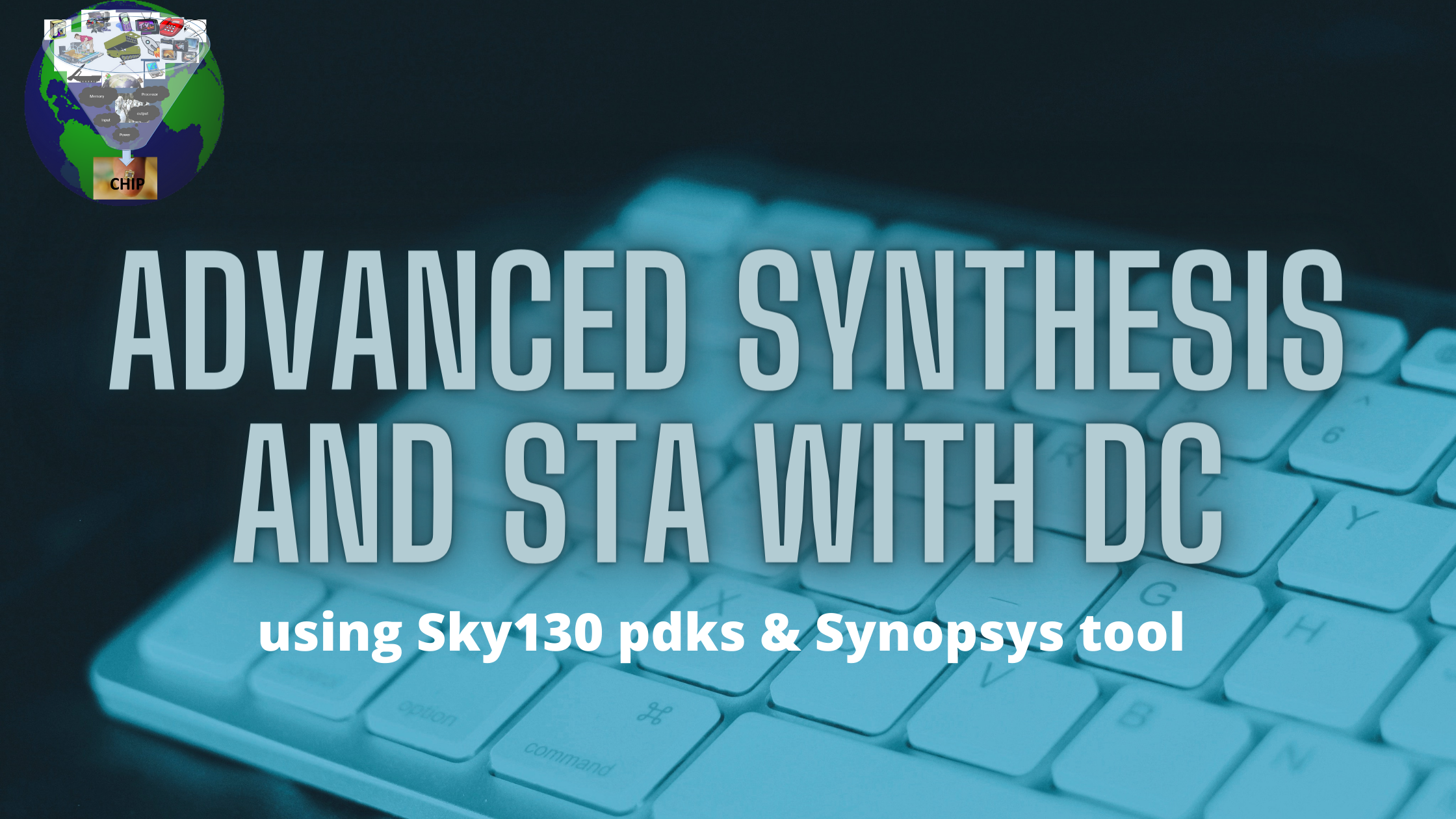 Advanced Synthesis and STA with Design Compiler – VLSI System Design
 How to Apply for Internship to get into VLSI Industry ? LIVE DEMO | QnA | EP-7 - YouTube
 fresherengineer - Twitter Search / Twitter
 Study On CCI Sizing Machine | PDF | Textiles | Materials
 VLSI QnA - Verilog Interview Questions - v1.4 Q.1) If a... | Facebook
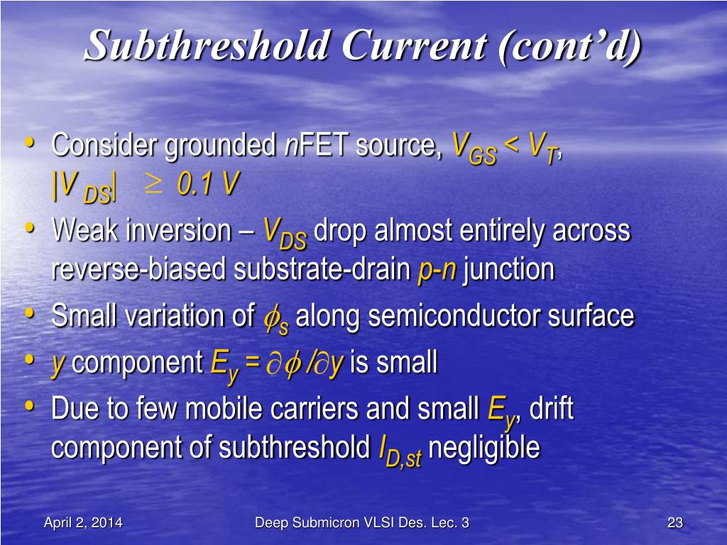 PPT - 332:578 Deep Submicron VLSI Design Lecture 3 Deep Sub-micron MOS Transistor Theory PowerPoint Presentation - ID:742777
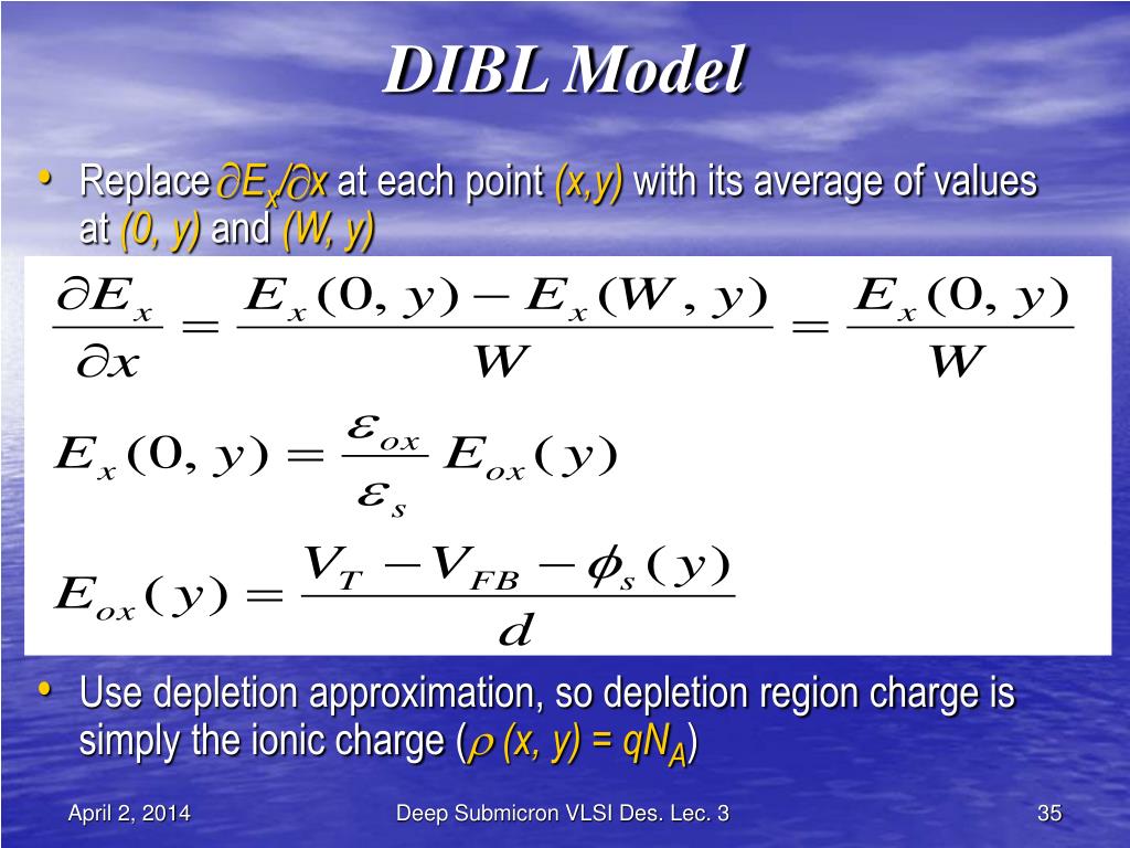 PPT - 332:578 Deep Submicron VLSI Design Lecture 3 Deep Sub-micron MOS Transistor Theory PowerPoint Presentation - ID:742777
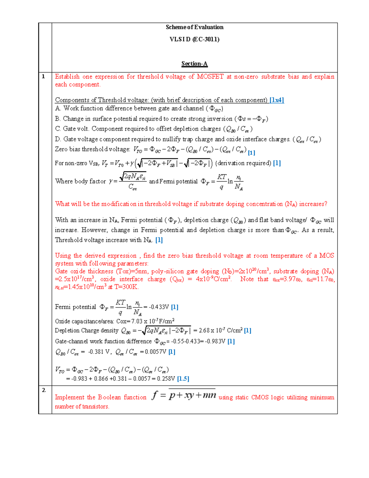 Question Paper sol - Scheme of Evaluation VLSI D (EC-3011) Section-A 1 Establish one expression for - StuDocu
 OGPV Course Information | PDF | Photovoltaics | Test (Assessment)
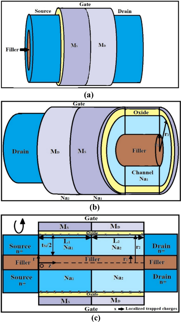 Gate Work Function-Engineered Graded-Channel Macaroni MOSFET: Exploration of Temperature and Localized Trapped Charge-Induced Effects with GIDL Analysis | SpringerLink
 Electrical And Electronics Engineers Career Opportunities In 2022
 Backend VLSI – VLSI Resources
 TechSimplifiedTV.in: TCL in VLSI
 FPGA – Fabric, Design and Architecture – VLSI System Design
 Exp 5 | PDF | Electronic Design | Digital Technology
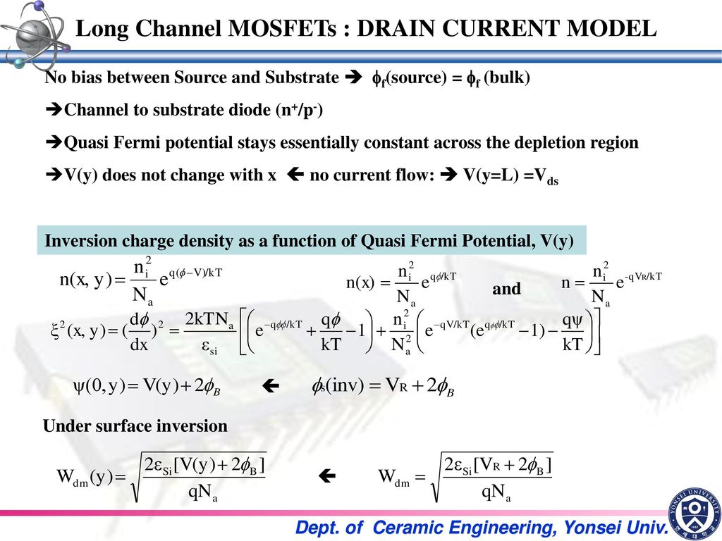 Long Channel MOSFETs. - ppt download
 If this doesn't make you expert, I will refund all your money...
 Cmos digital integrated circuit | Thesis Very large scale integration (VLSI) | Docsity
 Tintern Abbey' As A Record of Wordsworth's Spiritual Growth Through Discernible Stages of Development | PDF
 PDF) Recent Advances in Device Simulation Using Standard Transport Models
 If this doesn't make you expert, I will refund all your money...
 VLSI QnA - Verilog Interview Questions - v1.4 Q.1) If a... | Facebook
 Principal Engineer Resume Samples | Velvet Jobs
 TEMAZEPAM AND OXAZEPAM (Perca Fluviatilis) | PDF | Benzodiazepine | Mass Spectrometry
 PDF) Analysis and Modeling of Depletion-Mode MOS Transistors
 Selecting the Optimal Inductor for Power Converter Applications - Electronics/Electrical (EE/EC/EX)
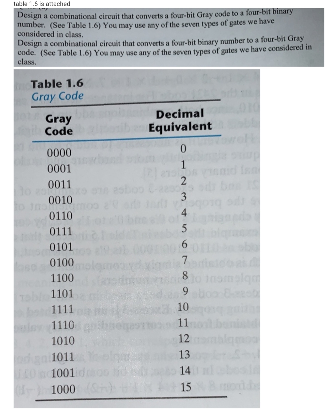 Answered: table 1.6 is attached Design a… | bartleby
 PERL Interview Questions for VLSI Jobs - Part 3 ~ TechSimplifiedTV.in
 CMOS Devices PN junctions and diodes NMOS and PMOS transistors - ppt download
 Review Ats | PDF | Clothing | Softlines (Retail)
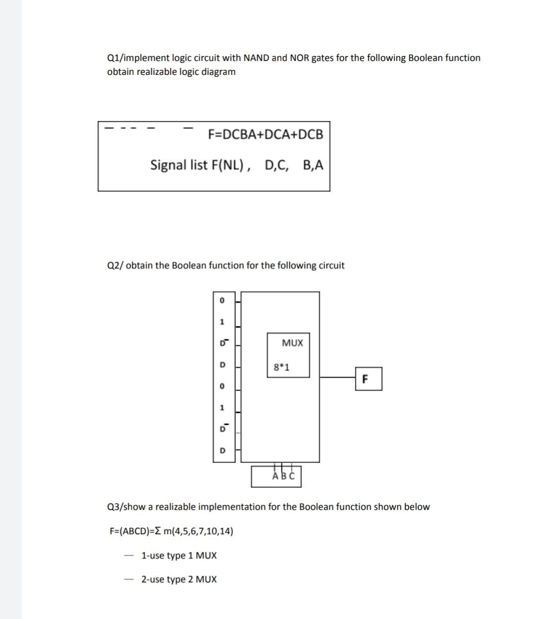 Answered: Q3/show a realizable implementation for… | bartleby
 bandu (@RummanMoe) / Twitter
 From PCB-Design to VLSI-Design Career Change ? Possible or Not ? QnA ! - YouTube
 PPT - 332:578 Deep Submicron VLSI Design Lecture 3 Deep Sub-micron MOS Transistor Theory PowerPoint Presentation - ID:742777
 If this doesn't make you expert, I will refund all your money...
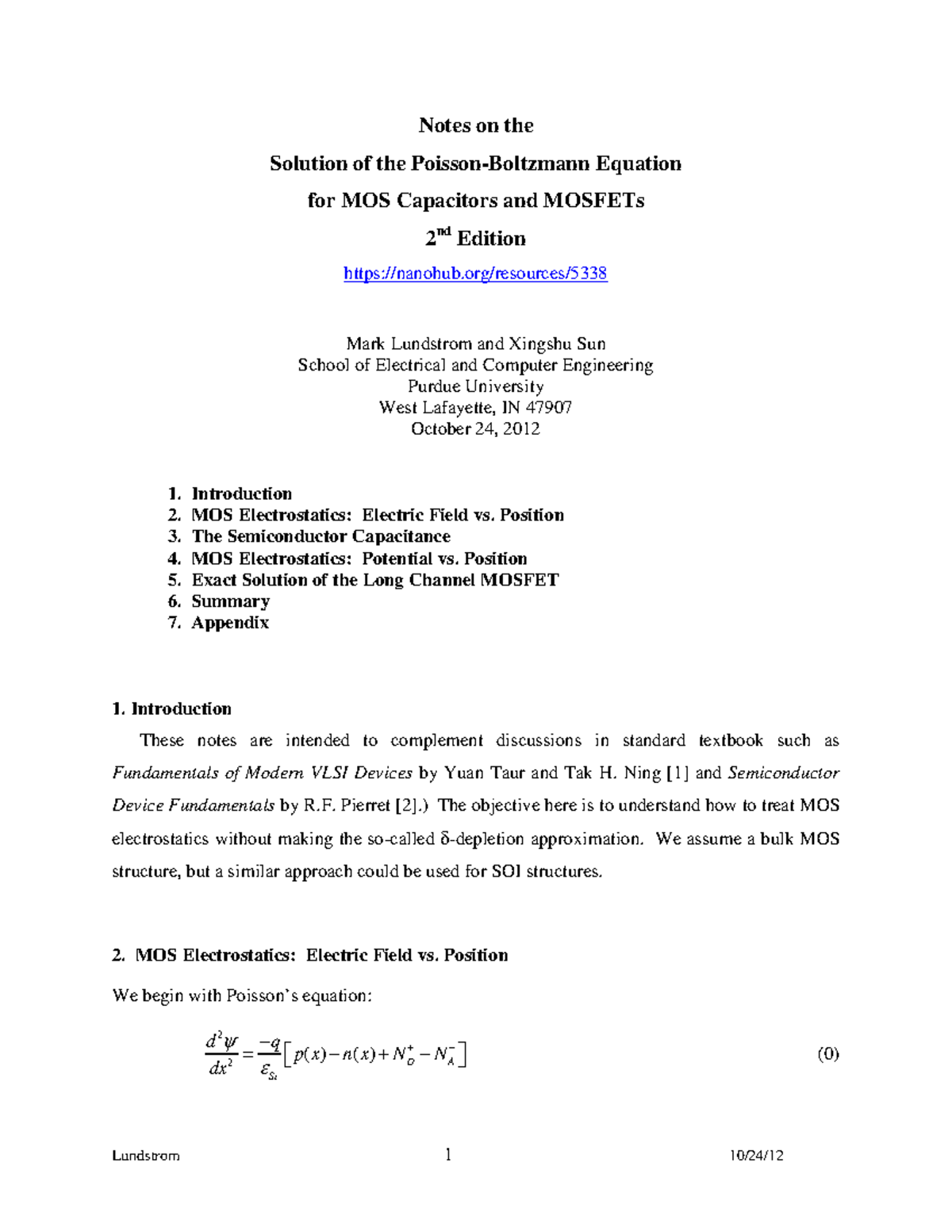 Exact MOS Solution - Notes on the Solution of the Poisson-Boltzmann Equation for MOS Capacitors and - StuDocu
 Answered: From the circuit below, determine… | bartleby
 Lecture 5 OUTLINE PN Junction Diodes I/V Capacitance Reverse Breakdown - ppt download
 11kv Voltage Regulator | PDF | Transformer | Insulator (Electricity)
 Top 25 Books For Electrical Engineers To Explore Things
 VSD-IAT – VLSI System Design
 UPSC CAPF (AC) 2022 DAF Released, Get Detailed Application Form @upsc.gov.in
 Shri Ramdeobaba College of Engineering and Management B.Tech Electrical Cutoff 2022: Check Closing Ranks for Previous Year | CollegeDekho
 BITSAT 2022 Iteration 3 seat allotment result out; check details here
 Top 23 Scrum Master Interview Questions and Answers
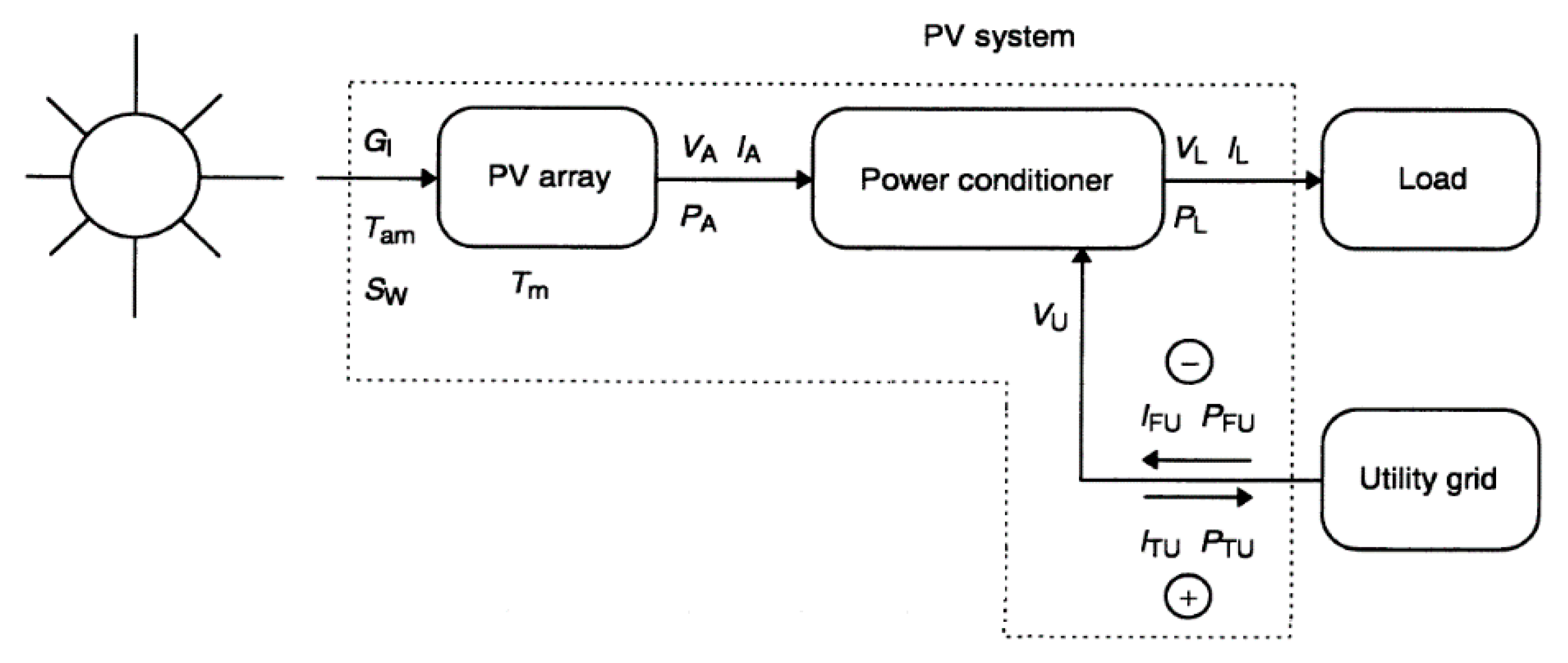 Electronics | Free Full-Text | PV Energy Performance in a Sustainable Campus | HTML
 Module 4.1 - Crosstalk or near-field coupling - Capacitive coupling, inductive coupling, common-impedance coupling - Electronics/Electrical (EE/EC/EX)
 Volvo Error Codes | PDF | Throttle | Turbocharger
 CMOS Devices PN junctions and diodes NMOS and PMOS transistors - ppt download
 QRcode - Twitter Search / Twitter
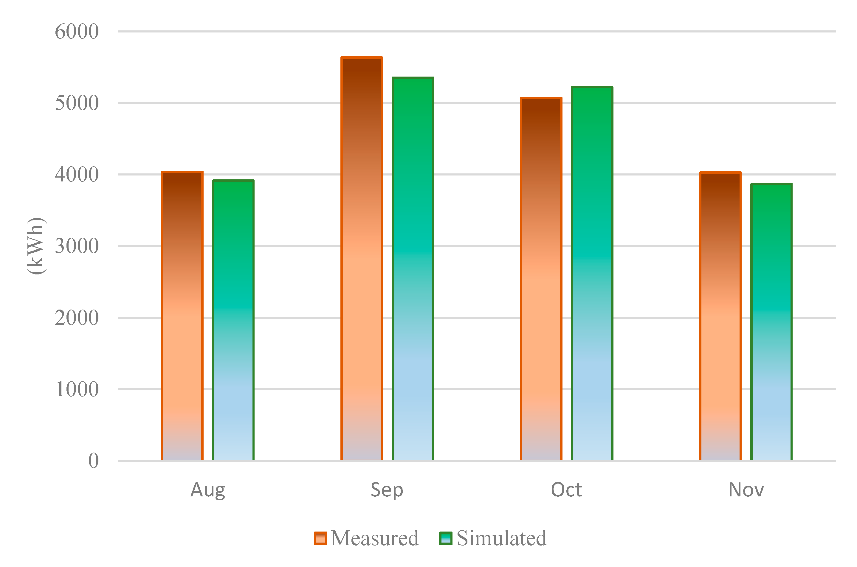 Electronics | Free Full-Text | PV Energy Performance in a Sustainable Campus | HTML
 IEEE EWU Student Branch | Dhaka | Facebook
Frequently Asked Questions
Is this DEVICE MODELING free to use?
Yes, 100% free. Download and print without creating an account or providing your email address.
What paper size does this template support?
Templates are designed for A4 and US Letter paper. Select 'Fit to page' in your printer dialog for the best fit.
Can I print multiple copies?
Yes. Once you download the image, you can print it as many times as you like for personal or educational use.