
PCB Object And Layer Transparency Features Altium
Download this free PCB Object And Layer Transparency Features Altium and use it right away. Optimized for A4 and Letter paper, all 35 designs are ready to print without editing software. No sign-up required.
How to Use This PCB Object And Layer Transparency Features Altium
- Browse the collectionScroll through the PCB Object And Layer Transparency Features Altium designs above and click any image to open it full size.
- Download the imageHit the Download button to save the full-resolution file to your device.
- Print on standard paperUse A4 or Letter paper. Select 'Fit to page' in your printer settings to ensure nothing is cut off.
- Use immediatelyNo editing, software, or account needed — it's ready the moment it comes out of the printer.
More Pcb Object And Layer Transparency Features Altium Templates
 Design Rules Available For PCB Layout In Altium Designer Altium
  Platzierungsanleitung F r Leiterplattenbauteile Altium
 Altium Default Clearance Between Polygon And Trace YouTube
 Altium Pcb Design Rules Pjawegreat
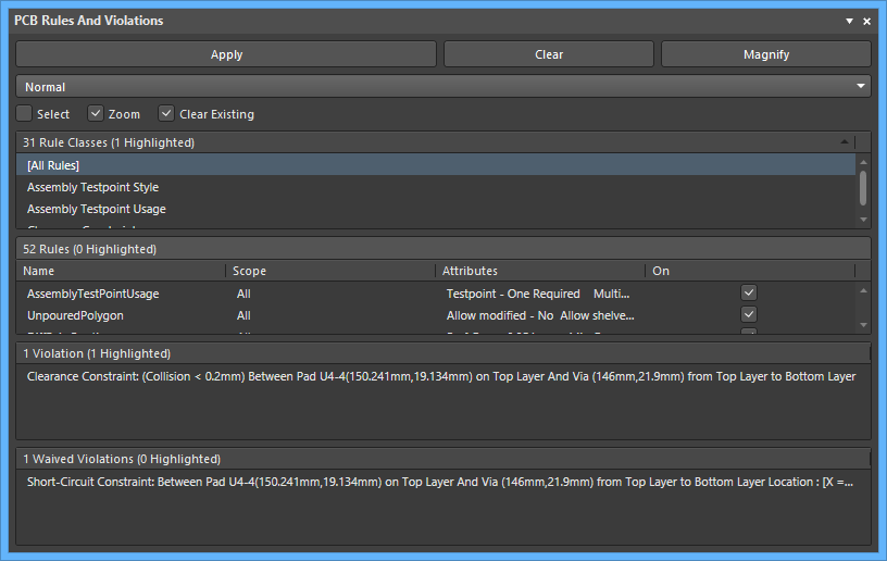 Browsing Design Constraints Issues Using The PCB Rules And Violations
  Top 5 PCB Design Rules You Need To Know PCB Design Blog Altium
 Streamlined Design Rule Editor Features ADSCvid Altium
 Altium Designer Altium Designer 22
  PCB Design Rules Visualization Features ADSCvid Altium
 Project Templates In A Workspace Connected To Altium Designer Altium
 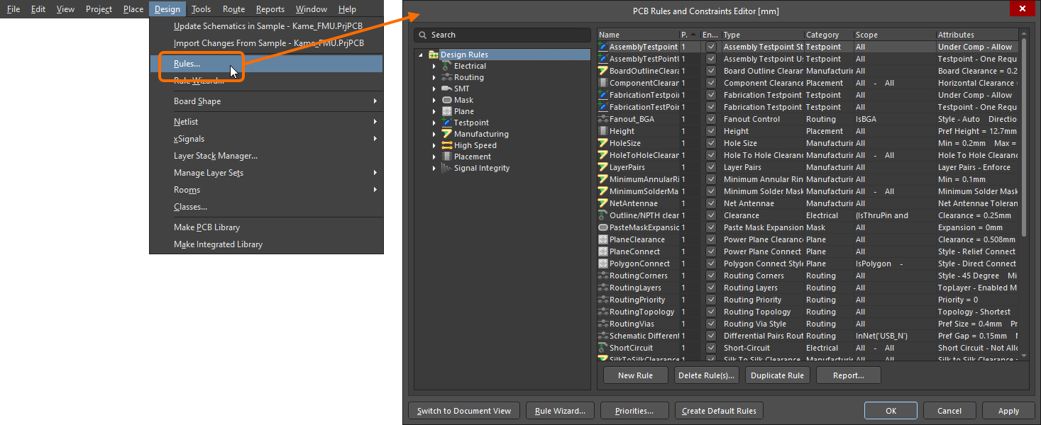 Design Rules Available For PCB Layout In Altium Designer Altium
 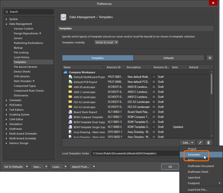 Creating A Schematic Template In Altium Designer Altium Designer 23
  Altium Default Visible Parameters In Sch Library YouTube
 How To Create Or Edit Existing PCB Template Title Block In Altium
  Electronics Altium Default Font YouTube
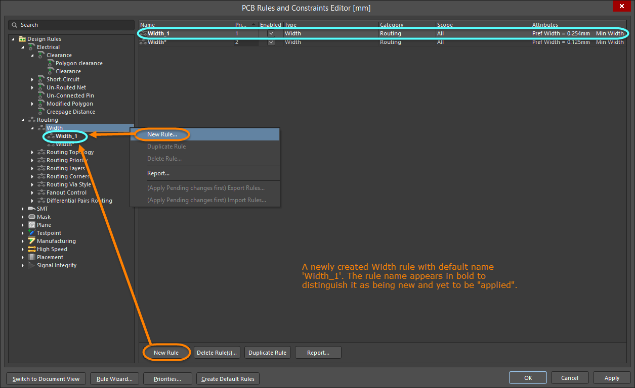 Defining Scoping Managing PCB Design Rules In Altium Designer
 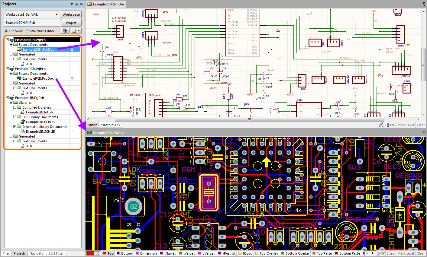 Altium Designer Log Files
 Online Documentation For Altium Products
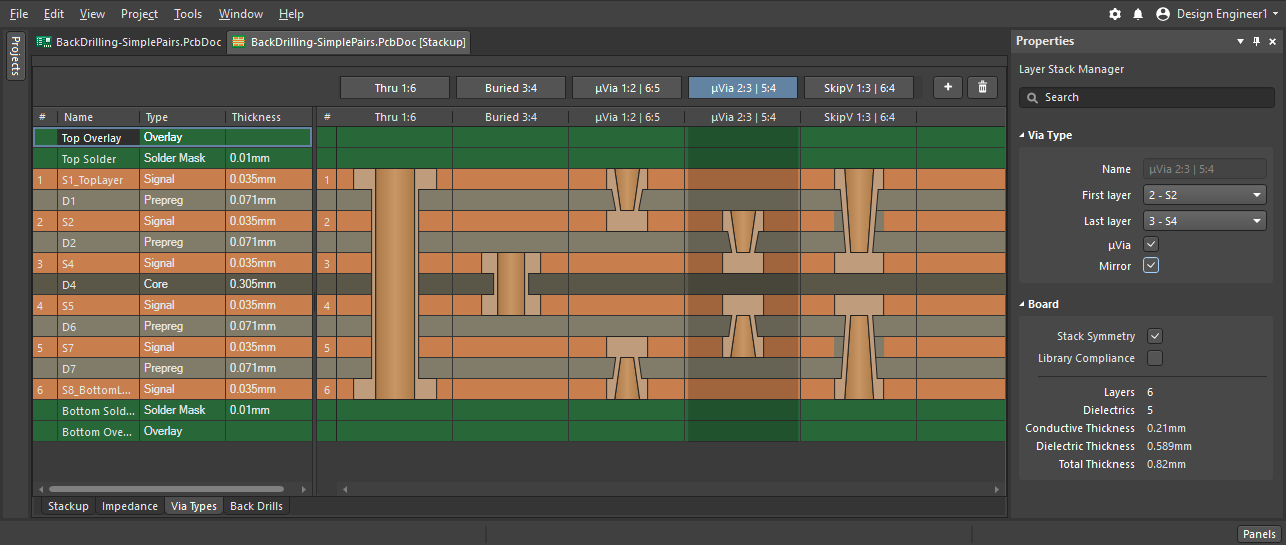 Defining The Via Types For Use With Your Board In Altium Designer
 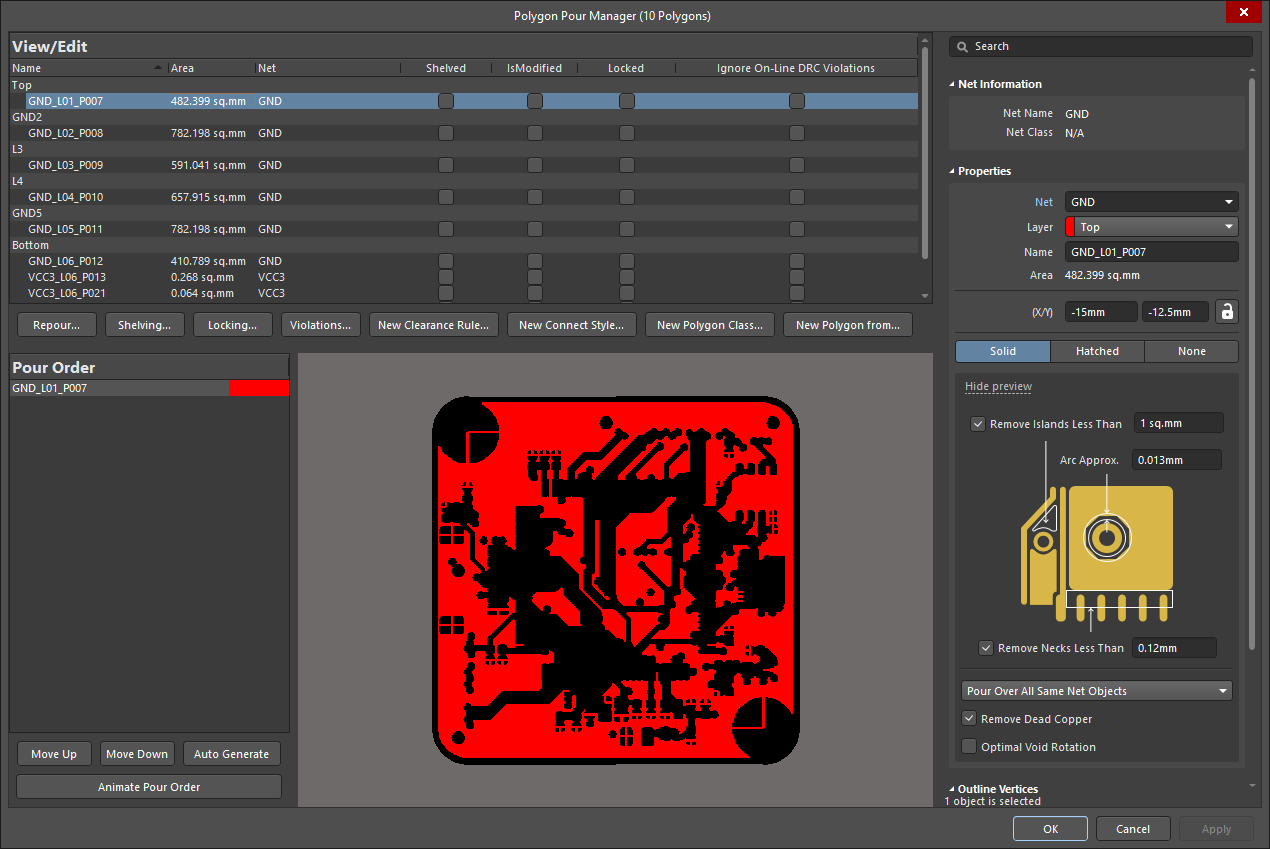 Polygon Pour Manager Altium Designer 22 User Manual Documentation
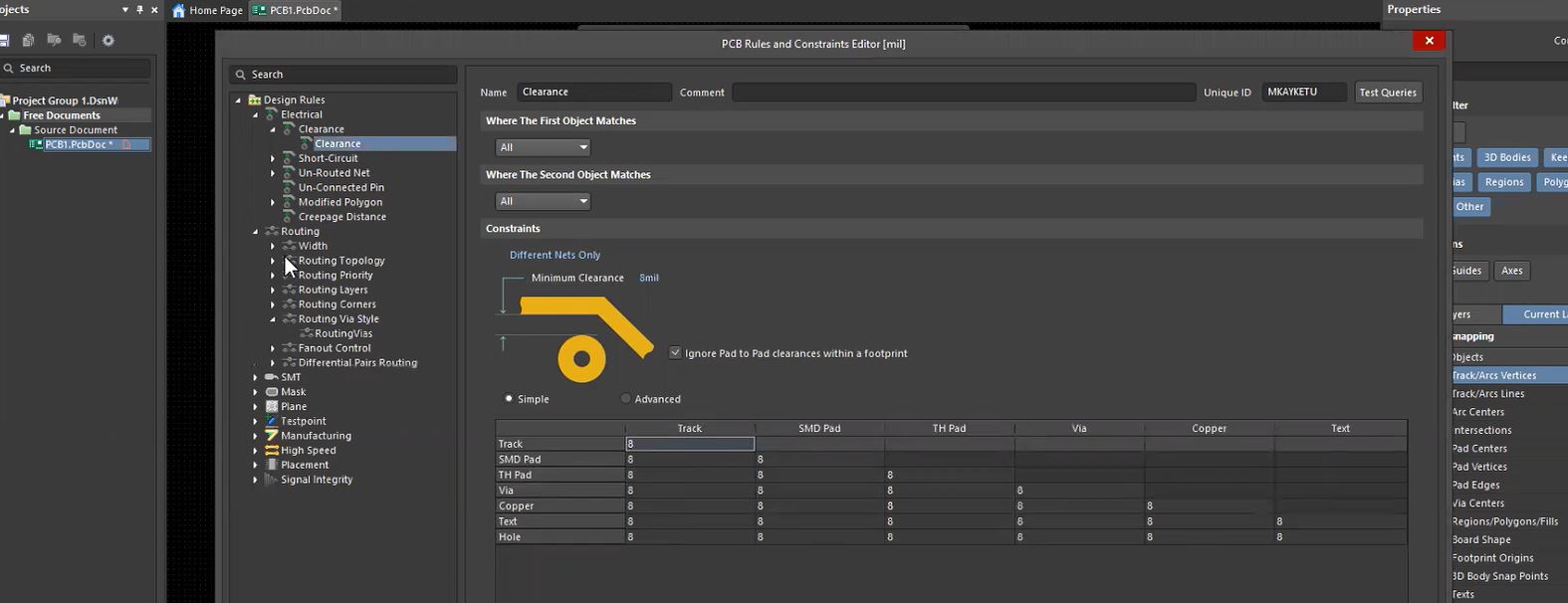 PCB Constraint Settings In Altium Designer And Allegro Sierra Circuits
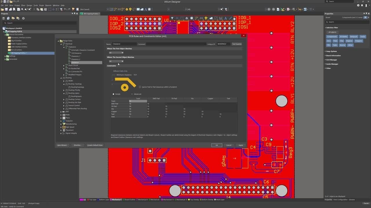 Altium Pcb Design Rules Qlerobest
 Creating A Schematic Template In Altium Designer Altium Designer 23
  Altium Design Rules PCB Circuits
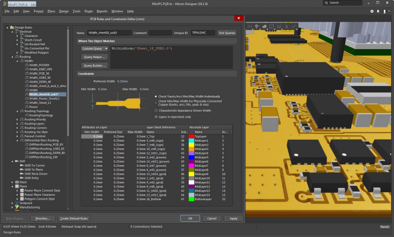 PCB Impedance Calculator And Stackup Design In Altium Designer
 SMD Pad Entry Rules Features ADSCvid Altium
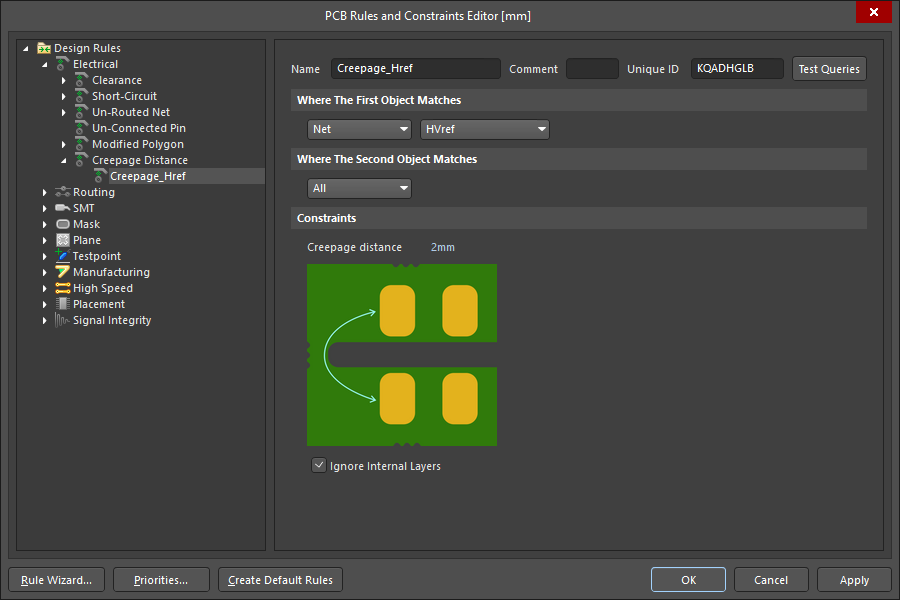 New PCB Design Rules New Feature Summary Altium Designer 20 0 User
  Altium Pcb Design Rules Drugxaser
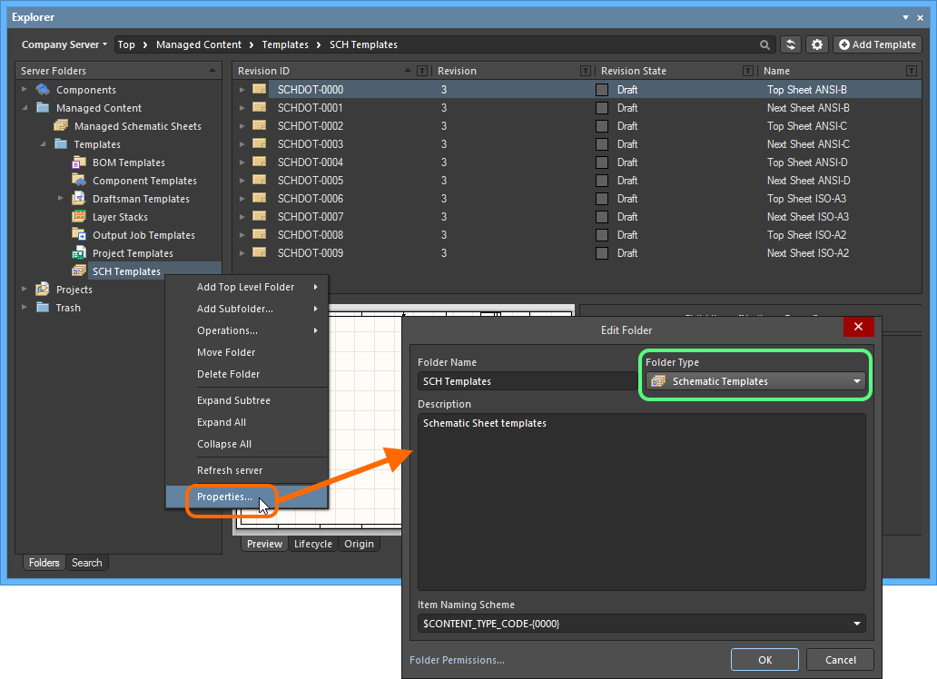 Schematic Templates In A Workspace Connected To Altium Designer
 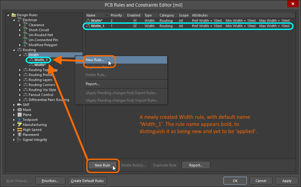 Defining Scoping Managing PCB Design Rules In Altium Designer
 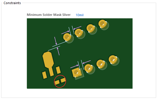 Working With The Minimum Solder Mask Sliver Design Rule On A PCB In PCB Object And Layer Transparency Features Altium
 Design Pcb Schematic And Layout In Altium By Sociallyvegan Fiverr
 Altium Pcb Design Rules Qlerobest
 Working With The Component Clearance Design Rule On A PCB In Altium
 Frequently Asked Questions
Is this PCB Object And Layer Transparency Features Altium free to use?
Yes, 100% free. Download and print without creating an account or providing your email address.
What paper size does this template support?
Templates are designed for A4 and US Letter paper. Select 'Fit to page' in your printer dialog for the best fit.
Can I print multiple copies?
Yes. Once you download the image, you can print it as many times as you like for personal or educational use.