Fpga Design Methodology
Download this free Fpga Design Methodology and use it right away. Optimized for A4 and Letter paper, all 35 designs are ready to print without editing software. No sign-up required.
 AN 584 Timing Closure Methodology For Advanced FPGA Altera
 Figure 2 From Design Preservation Methodology Based On FPGA Semantic
  Figure 1 From FPGA Implementation Of SRAM Redundancy Methodology Using
  Xilinx FPGA Pin Planning Methodology
  PDF FPGA Design Methodology For Industrial Control Systems A Review
  Top down Design Methodology With A View To Designing Simulating And
  Standard Cell ASIC To FPGA Design Methodology And
Standard Cell ASIC To FPGA Design Methodology And FPGA Design Easics
 SDAccel Based FPGA Design Methodology Flow Download Scientific Diagram
 FPGA Vs ASIC HardwareBee
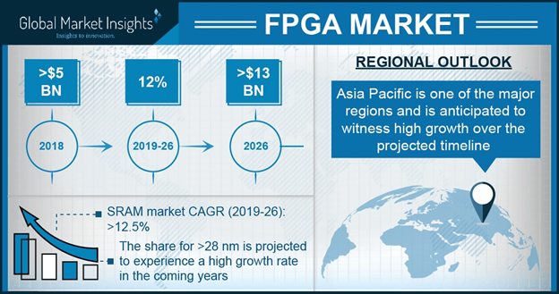 Field Programmable Gate Array FPGA Market Share 2019 2026 Forecasts
 Ren Richter Used Books Rare Books And New Books BookFinder
 VSIPL FPGA Design Methodology
VSIPL FPGA Design Methodology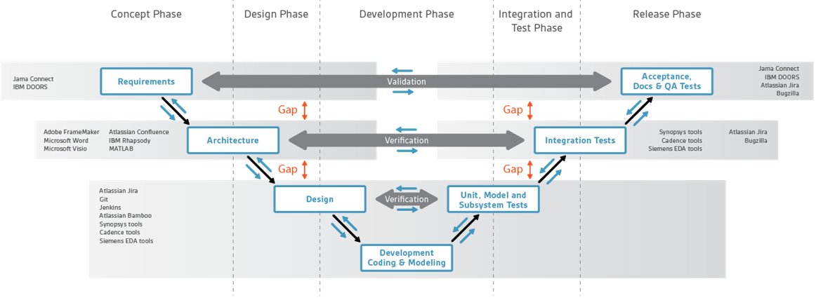 Reinventing Traceability Adding Domain Intelligence With Arteris
  A Hardware software Partition Methodology Targeted To An FPGA CPLD
 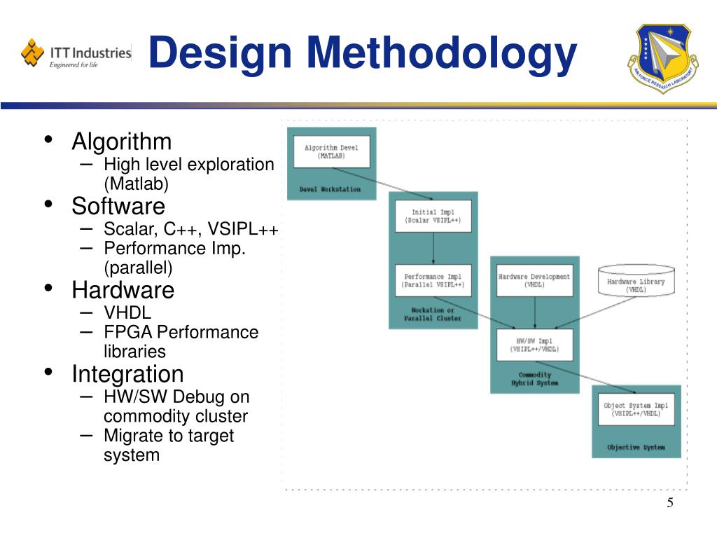 PPT VSIPL FPGA Design Methodology PowerPoint Presentation Free
  Xilinx Vivado Maker hub
 Xilinx Design Reuse Methodology For ASIC And FPGA Designers
 Typical FPGA Design Flow Download Scientific Diagram
 Linear CCD Based Spectrometry Using Either An ASIC Or FPGA Design
  New Design methodology Of High performance TDC On A Low Cost FPGA Targets
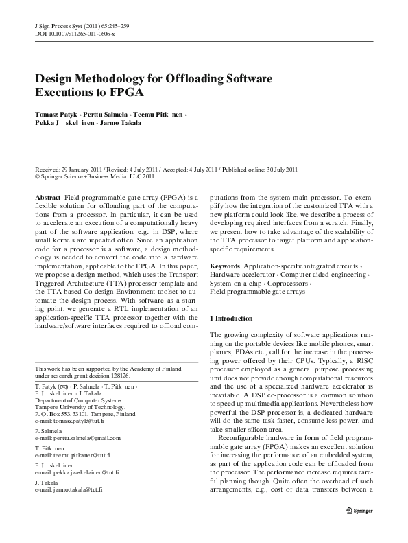 PDF Design Methodology For Offloading Software Executions To FPGA
  Very Large Scale Integration VLSI FPGA Implementation Design Cycle
 A Structured Methodology For System on an FPGA Design
 BaySand Introduces Enhanced FPGA To ASIC Conversion Program With IP
  Digitronix Nepal 4th National FPGA Design Competition 2019
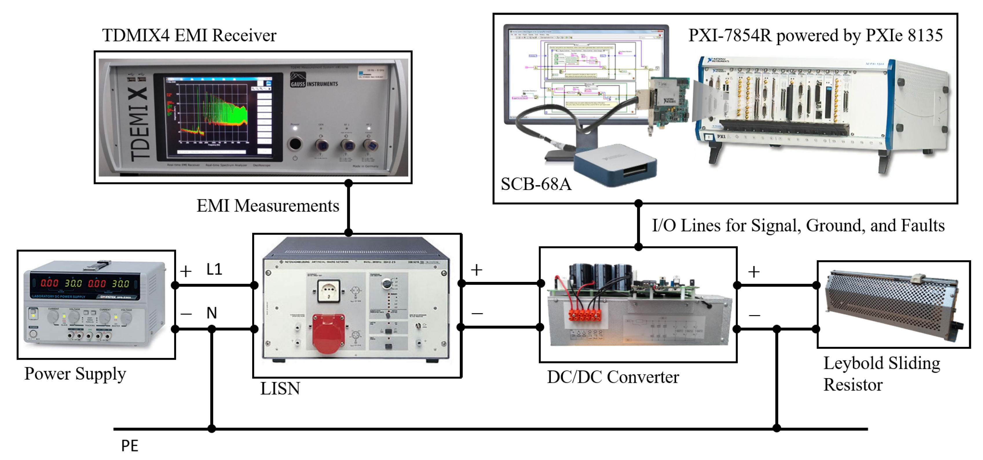 Energies Free Full Text FPGA Based System For Electromagnetic
  Design Methodology Of FPGA Download Scientific Diagram
 Deep Learning Hardware FPGA Vs GPU
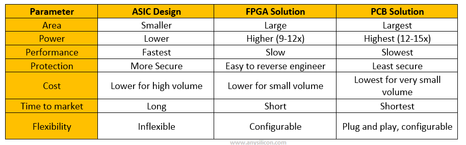 When And Why Should You Choose An ASIC AnySilicon
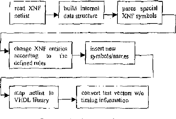 Figure 1 From FPGA To ASIC Conversion Design Methodology With The
  Design Methodology With System Generator In Simulink Of A FHSS
  Select The Correct Debug Methodology For Your Altera FPGA Design
 FPGA Design Methodology